


Another significant period was spent at KAUST(Dec 2021-May 2025), where I never felt bored during work. I led and executed several research projects and had the opportunity to expand my expertise across various research fields.
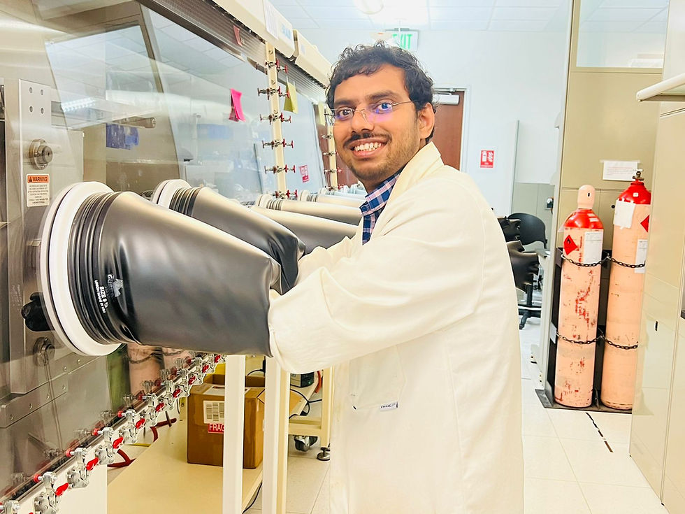
Enjoying hands-on work while utilising the KAUST Nanofabrication Lab facilities.
I spent a significant and memorable period of my life pursuing my Ph.D. (2014–2020), marked by invaluable experiences and enduring memories.
Another significant period was spent at KAUST(Dec 2021-May 2025), where I never felt bored during work. I led and executed several research projects and had the opportunity to expand my expertise across various research fields.
Expertise in Research Field
-
Organic Electronics
-
Device Physics (Diode and Thin Film Transistors)
-
Sensors and Detectors
-
Energy Harvesting Device
-
Nanotechnology (Nanostructure, Nanomaterial, Nanogaps)
-
Flexible and Wearable Device
-
Materials Engineering (SAM modification, nanocomposites, doping, etc.)
Key Achievements
PhD
-
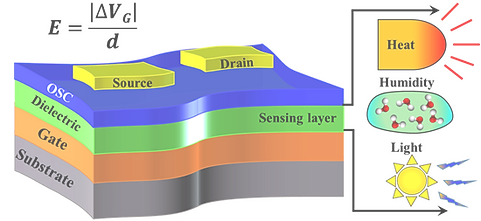
Gained expertise in organic electronic devices and developed a novel sensing approach using the dielectric layer of OFETs as the sensing medium without compromising low operating voltage; demonstrated highly responsive sensing to heat, humidity, and light, with tunability via high gate electric fields.
-
Designed and validated moisture-induced energy harvesting devices with integrated functionality as self-biased humidity sensors.
-
Developed silver nanorod-based strain sensors for advanced biomedical applications, including blood profile monitoring and robotic skin.
Pictures of Sensors Developed During PhD
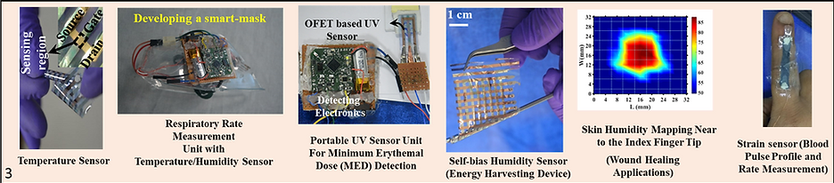
A spirometer based on the temperature sensor is currently undergoing clinical trials in India
Post PhD
-
At University College London (UCL), I developed high-k polymer nanocomposites for cost-effective, high-resolution display technologies by introducing a novel concept of functionalized hetero-phase filler-based composites to enhance dielectric properties and achieve a high dielectric constant.
-
Gained expertise in functional chemistry by modifying nanoparticles using self-assembled monolayers (SAMs).

-
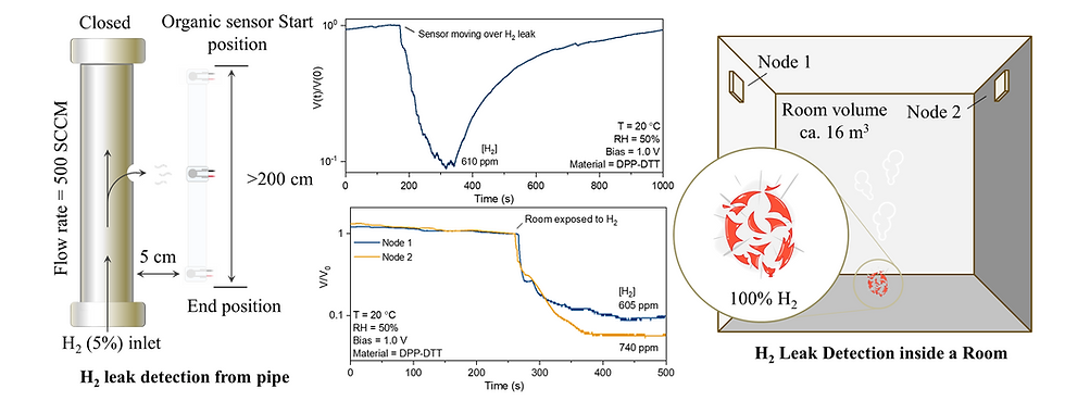
At KAUST, observed a phenomenon in organic semiconductors known as the oxygen doping and hydrogen de-doping cycle, and leveraged it to develop a highly responsive, selective, and fast organic hydrogen sensor.
-
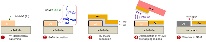
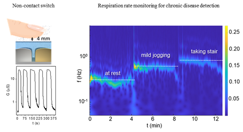
Developed ultra-fast humidity sensors using biopolymers as the active sensing layer in nanogap-based devices, fabricated through a scalable adhesion lithography method, and demonstrated their application in non-contact switches and respiratory monitoring.
-
Exploring polarization effects in OFET dielectric materials to improve device performance for memory and logic circuit applications.
Organic Hydrogen Sensor and Sensing Mechanism

Demonstrations of Organic Hydrogen Sensor

Process steps for adhesion lithography-based nanogap fabrication
Nanogap based ultra-fast Organic humidity Sensor
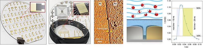
Demonstration of applications of the ultra-fast humidity sensor
Research Laboratory Setup
PhD (2014-2020)
-
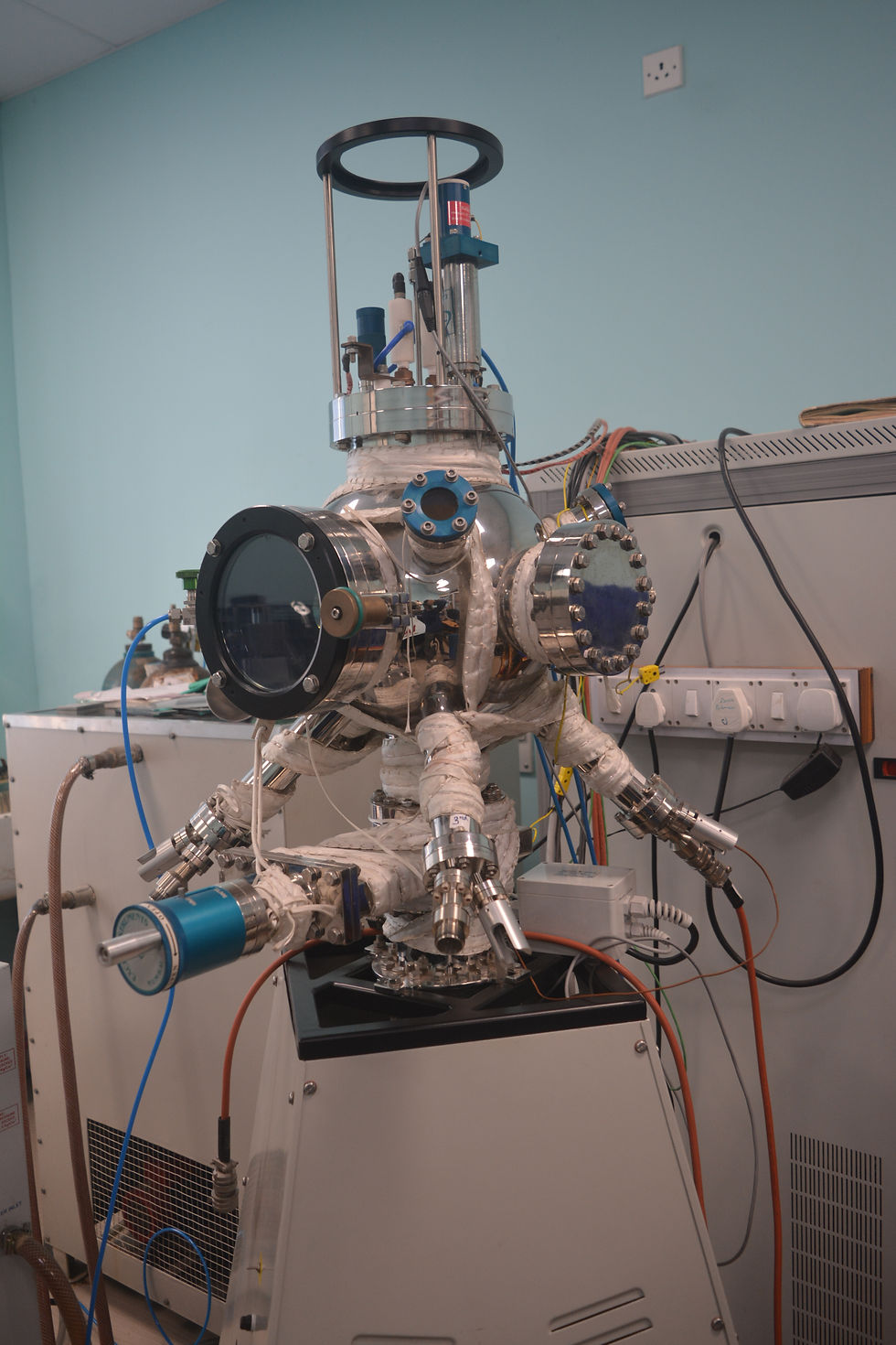
Organic Molecular Beam Deposition System: Installed and optimised for precise thin-film growth of organic semiconducting materials such as Pentacene, Copper Phthalocyanine, Cobalt Phthalocyanine, DNTT, and C8BTBT through controlled sublimation.
-
Physical Vapour Deposition (PVD) System: Configured for the fabrication of organic nanowires and nanorods using thermal sublimation techniques with various organic semiconductors.
-
Anodization Setup: Developed and integrated for controlled electrochemical oxidation processes used in dielectric layer formation and surface treatment.
-
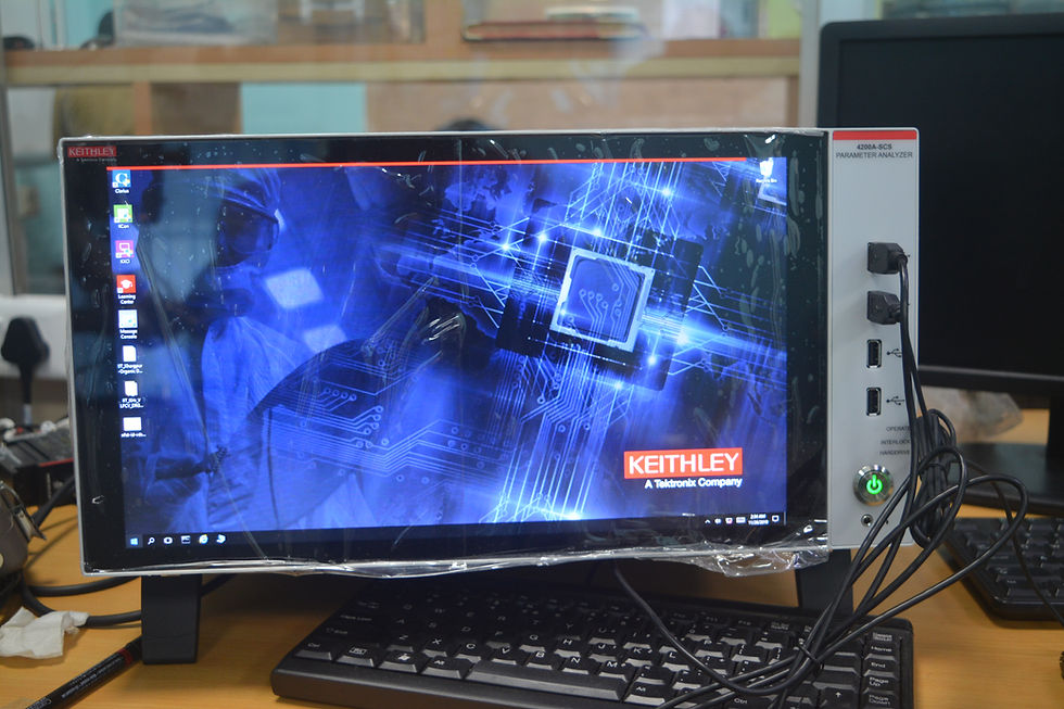
OFET Characterisation Platform: Established a measurement setup using probe stations and Source Measurement Units (SMUs) for electrical characterisation of organic field-effect transistors.
-
Dielectric Property Measurement System: Set up using a Capacitance Measurement Unit (CMU) to evaluate the dielectric constant, loss tangent, and frequency-dependent behaviour of insulating materials.
-
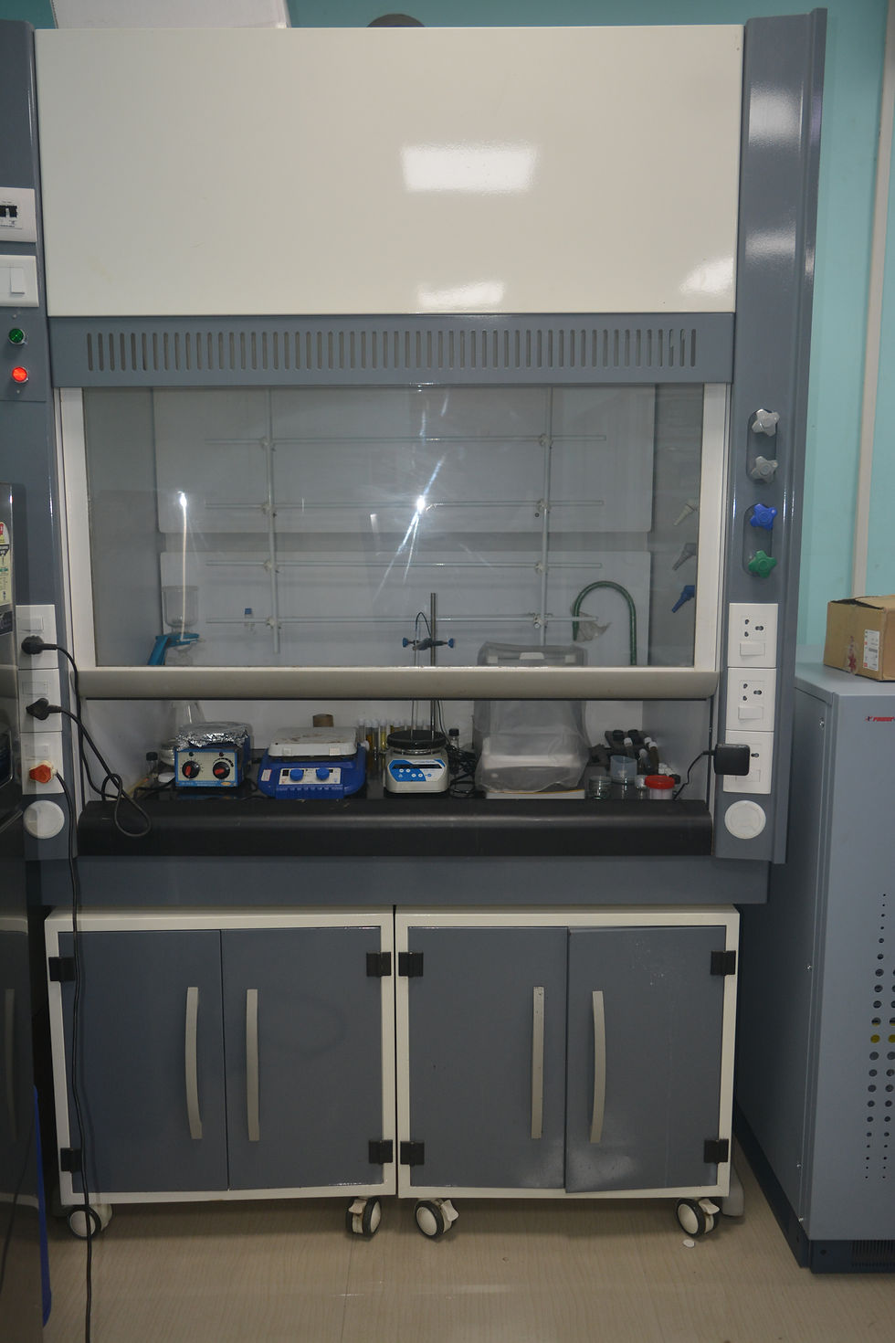
Custom Humidity Sensing Setup: Designed and fabricated an environmental control chamber with integrated sensors and data acquisition for accurate humidity response studies.
-
Strain Sensing Measurement Setup: Constructed a platform to test and calibrate strain sensors under various mechanical deformations, suitable for wearable and flexible electronics research.
Post-PhD (2020-2025)
-
Dielectric Measurement Setup at UCL: Developed a system to characterise high-k polymer nanocomposites for dielectric property evaluation.
-
Humidity Sensing Setup at KAUST: Designed and built a controlled humidity sensing system integrated with a MATLAB interface for real-time data acquisition and analysis.
-
Hydrogen Sensing Setup at KAUST: Developed a custom hydrogen sensing platform with precise gas flow control and a MATLAB-based interface for testing under various environmental conditions.
-
Porous Film Fabrication Setup: Implemented the Breath Figure Method to fabricate porous thin films with controllable morphology for sensor applications.
-
CMOS Circuit Measurement Setup: Characterised organic CMOS inverters under diverse environmental and electrical conditions.
Experience: Gained hands-on experience in using the synchrotron facility at the Indian Beamline (BL18B), Photon Factory, KEK, Japan.
Hands on Experience during PhD work
Describe your image
Describe your image
Hands on Experience during Post-PhD work


Describe your image

Describe your image